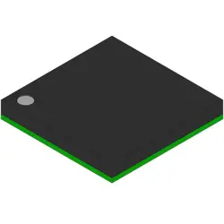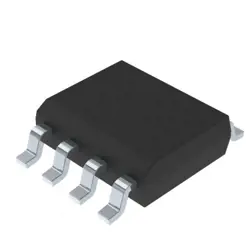
Hình ảnh chỉ để tham khảo
W25Q64FVSIG
- Nhà sản xuất
- Ông. Phần #W25Q64FVSIG
- Gói
- Bảng dữ liệu
- Có sẵn28190
100% gốc & amp; Mới
24 giờ sẵn sàng để vận chuyển
Bảo hành 365 ngày
RFQ & amp; Nhận thêm Giảm giá
Thông số kỹ thuật
| Manufacturer | JLCPCB Assembly |
| Package | SOP-8 |
Tổng quan
Description
Key features include:
- Voltage: Operates typically at 2.7V to 3.6V, making it suitable for low-power applications.
- Data retention: Can maintain data for up to 20 years under proper conditions.
- Erase cycles: Supports up to 100,000 program/erase cycles per block.
- Package types: Available in various packages, including SOIC and WSON, making it versatile for different design needs.
The W25Q64FVSIG is widely used in embedded systems, consumer electronics, automotive applications, and IoT devices due to its reliability and performance.
Features
- Interface: SPI (Serial Peripheral Interface) with support for dual and quad I/O modes for higher data transfer rates.
- Speed: Offers a maximum clock frequency of 104 MHz in quad mode.
- Density: 64Mb (8MB) storage capacity.
- Voltage Range: Operates at a voltage of 2.7V to 3.6V.
- Endurance: Supports 100,000 program/erase cycles per sector.
- Data Retention: Data retention period of up to 20 years.
- Sector Architecture: Organized into 256 sectors of 64KB each.
- Commands: Supports various commands for read, program, erase, and other functions.
- Chip Erase: Fast chip erase functionality for quick data management.
- Package: Available in a small, compact 8-pin SOP package.
This chip is widely used in applications such as consumer electronics, automotive, and communication devices for firmware storage and data retention.
Package
Pinout
Pin Count and Functions:
1. CS (Chip Select) - Controls the selection of the chip.
2. SO (Serial Output) - Data output pin for transmitting data from the memory to the host.
3. SI (Serial Input) - Data input pin for receiving data from the host.
4. SCK (Serial Clock) - Clock input for synchronizing data transfers.
5. WP (Write Protect) - Active low pin for write protection.
6. HOLD - Pauses serial communication without resetting the chip.
7. VCC - Power supply pin.
8. GND - Ground pin.
9. RESET - Optional reset pin (if implemented).
The remaining pins are used for specific features or are reserved. The chip operates via SPI (Serial Peripheral Interface) and supports various modes for reading, writing, and erasing data.
Manufacturer
Application
Equivalent
Vận chuyển
Phương pháp vận chuyển Chúng tôi
cung cấp dịch vụ vận chuyển toàn cầu thông qua DHL, FedEx, TNT, UPS hoặc bất kỳ nhà giao hàng khác mà bạn lựa chọn.
Tham khảo phí vận chuyển (DHL / FedEx):
Hãng DHL: Chi phí vận chuyển dao động từ $ 25- $ 45 (0,5kg), với thời gian giao hàng ước tính là 2-5 ngày làm việc.
FedEx: Chi phí vận chuyển dao động từ $ 25- $ 40 (0,5kg), với thời gian giao hàng ước tính là 3-7 ngày làm việc.
Sản phẩm UPS: Chi phí vận chuyển dao động từ $ 25- $ 45 (0,5kg), với thời gian giao hàng ước tính là 3-7 ngày làm việc.
TNT: Chi phí vận chuyển dao động từ $ 25- $ 65 (0,5kg), với thời gian giao hàng ước tính là 3-7 ngày làm việc.
EMS: Chi phí vận chuyển dao động từ $ 30- $ 50 (0,5kg), với thời gian giao hàng ước tính là 7-15 ngày làm việc.
Đăng ký Air Mail: Chi phí vận chuyển là $ 2- $ 4 (0.1kg), với thời gian giao hàng ước tính là 5-20 ngày làm việc.
Thanh toán
Payment Methods
Thời hạn thanh toán là 100% trả trước.
Hiện tại, chúng tôi chỉ chấp nhận các phương thức thanh toán dưới đây:
1. PayPal
2. Thẻ tín dụng / ghi nợ
3. Chuyển dây
Tương tự
-
![MX25L3233FM1I-08Q]() MX25L3233FM1I-08Q
MX25L3233FM1I-08Q
Macronix
-
![MX29F400CBTI-70G]() MX29F400CBTI-70G
MX29F400CBTI-70G
Macronix
-
![MX66U1G45GXDI00]() MX66U1G45GXDI00
MX66U1G45GXDI00
Macronix
-
![MX25V5126FM1I]() MX25V5126FM1I
MX25V5126FM1I
Macronix
-
![MX25V4035FZUI]() MX25V4035FZUI
MX25V4035FZUI
Macronix
-
![MX25R3235FZNIL0]() MX25R3235FZNIL0
MX25R3235FZNIL0
Macronix
-
![MX25L8035EM2I-10G]() MX25L8035EM2I-10G
MX25L8035EM2I-10G
Macronix
-
![MX25L25673GMI-10G]() MX25L25673GMI-10G
MX25L25673GMI-10G
Macronix
-
![MX29GL512FHXFI-11G]() MX29GL512FHXFI-11..
MX29GL512FHXFI-11..
Macronix
-
![MX25U25643GZNI00]() MX25U25643GZNI00
MX25U25643GZNI00
Macronix
-
![MX25V1635FM2I]() MX25V1635FM2I
MX25V1635FM2I
Macronix
-
![MX25U6435FM2I-10G]() MX25U6435FM2I-10G
MX25U6435FM2I-10G
Macronix