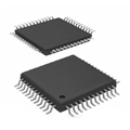
Hình ảnh chỉ để tham khảo
RMLV1616AGSA-5S2#AA0
IC SRAM 16MBIT PARALLEL 48TSOP I
- Nhà sản xuất
- Ông. Phần #RMLV1616AGSA-5S2#AA0
- Gói TFSOP-48
- Bảng dữ liệu
- Có sẵn3339
100% gốc & amp; Mới
24 giờ sẵn sàng để vận chuyển
Bảo hành 365 ngày
RFQ & amp; Nhận thêm Giảm giá
Thông số kỹ thuật
| Package | Tray |
| ProductStatus | Active |
| MemoryType | Volatile |
| MemoryFormat | SRAM |
| Technology | SRAM |
| MemorySize | 16Mb (2M x 8, 1M x 16) |
| MemoryInterface | Parallel |
| WriteCycleTime-WordPage | 55ns |
| AccessTime | 55 ns |
| Voltage-Supply | 2.7V ~ 3.6V |
| OperatingTemperature | -40°C ~ 85°C (TA) |
| MountingType | Surface Mount |
| Package/Case | 48-TFSOP (0.724, 18.40mm Width) |
Tổng quan
Description
Key features typically include a wide voltage range, low access times, and compatibility with standard memory interfaces. This makes it suitable for applications requiring quick data retrieval and storage. Additionally, the "AGSA" in the part number may refer to specific manufacturing or performance standards.
For detailed specifications, including pin configuration, operating conditions, and application notes, it is recommended to consult the manufacturer’s datasheet directly.
Features
1. Memory Density: 16 megabits (2MB).
2. Data Width: 16 bits, allowing for efficient data handling.
3. Access Time: Fast access times, enhancing performance in time-critical applications.
4. Operating Voltage: Typically operates at 3.3V, which is low-power and suitable for battery-operated devices.
5. Temperature Range: Designed for reliable operation across a wide temperature range.
6. Asynchronous Operation: No need for external clocking, simplifying design and integration.
7. Low Power Consumption: Ideal for energy-efficient applications.
This SRAM is commonly used in telecommunications, networking, and various consumer electronics, providing reliable and quick data storage solutions.
Package
Pinout
- Data Bus: 8 pins (D0-D7) for data input/output.
- Address Inputs: 17 pins (A0-A16) for addressing the memory locations.
- Chip Enable (CE): 1 pin to activate the memory chip.
- Write Enable (WE): 1 pin to control write operations.
- Output Enable (OE): 1 pin to control output data access.
- VSS: 1 pin for ground connection.
- VCC: 1 pin for power supply.
This chip operates at a supply voltage of 5V and is designed for high-speed applications.
Manufacturer
Application
Equivalent
Vận chuyển
Phương pháp vận chuyển Chúng tôi
cung cấp dịch vụ vận chuyển toàn cầu thông qua DHL, FedEx, TNT, UPS hoặc bất kỳ nhà giao hàng khác mà bạn lựa chọn.
Tham khảo phí vận chuyển (DHL / FedEx):
Hãng DHL: Chi phí vận chuyển dao động từ $ 25- $ 45 (0,5kg), với thời gian giao hàng ước tính là 2-5 ngày làm việc.
FedEx: Chi phí vận chuyển dao động từ $ 25- $ 40 (0,5kg), với thời gian giao hàng ước tính là 3-7 ngày làm việc.
Sản phẩm UPS: Chi phí vận chuyển dao động từ $ 25- $ 45 (0,5kg), với thời gian giao hàng ước tính là 3-7 ngày làm việc.
TNT: Chi phí vận chuyển dao động từ $ 25- $ 65 (0,5kg), với thời gian giao hàng ước tính là 3-7 ngày làm việc.
EMS: Chi phí vận chuyển dao động từ $ 30- $ 50 (0,5kg), với thời gian giao hàng ước tính là 7-15 ngày làm việc.
Đăng ký Air Mail: Chi phí vận chuyển là $ 2- $ 4 (0.1kg), với thời gian giao hàng ước tính là 5-20 ngày làm việc.
Thanh toán
Payment Methods
Thời hạn thanh toán là 100% trả trước.
Hiện tại, chúng tôi chỉ chấp nhận các phương thức thanh toán dưới đây:
1. PayPal
2. Thẻ tín dụng / ghi nợ
3. Chuyển dây
Tương tự
-
![MX29F400CBTI-70G]() MX29F400CBTI-70G
Macronix
-
![MX66U1G45GXDI00]() MX66U1G45GXDI00
Macronix
-
![MX25V2033FM1I]() MX25V2033FM1I
Macronix
-
![MX25V16066M1I02]() MX25V16066M1I02
Macronix
-
![MX25V16066M2I02]() MX25V16066M2I02
Macronix
-
![MX30LF2G28AD-TI]() MX30LF2G28AD-TI
Macronix
-
![MX29GL512FHXFI-11G]() MX29GL512FHXFI-11..
Macronix
-
![MX25U51279GXDR00]() MX25U51279GXDR00
Macronix
-
![MX25V1635FM2I]() MX25V1635FM2I
Macronix
-
![MX25U3232FZBI02]() MX25U3232FZBI02
Macronix
-
![MX25L6433FM2I-08G]() MX25L6433FM2I-08G
Macronix
-
![MX25L12833FM2I-10G]() MX25L12833FM2I-10..
Macronix