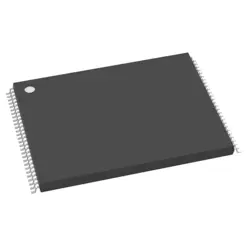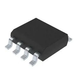
Hình ảnh chỉ để tham khảo
HEF4011BT
Logic Gates
- Nhà sản xuất
- Ông. Phần #HEF4011BT
- Gói
- Bảng dữ liệu
- Có sẵn5679
100% gốc & amp; Mới
24 giờ sẵn sàng để vận chuyển
Bảo hành 365 ngày
RFQ & amp; Nhận thêm Giảm giá
Thông số kỹ thuật
Tổng quan
Description
This IC is known for its low power consumption, high noise immunity, and compatibility with other CMOS devices. It is commonly used in digital logic circuits, signal processing, and switching applications. The package typically features a DIP (Dual In-line Package) or surface mount options, making it suitable for prototyping and production.
In summary, the HEF4011BT is essential for implementing NAND logic functions in electronic designs, providing flexibility and efficiency in various applications.
Features
1. Quad NAND Gates: Contains four independent two-input NAND gates.
2. Wide Supply Voltage Range: Operates from 3V to 15V, making it versatile for various applications.
3. Low Power Consumption: Consumes less power compared to other logic families, enhancing energy efficiency.
4. High Noise Immunity: Offers good noise margins, ensuring reliable operation in noisy environments.
5. Complementary Output: Provides both high and low output signals, suitable for driving subsequent stages.
6. Standard Logic Levels: Compatible with standard TTL logic levels.
7. Temperature Range: Operates effectively over a wide temperature range (-40°C to +125°C).
8. Package Options: Available in various package types, including DIP, SOIC, and TSSOP.
This makes the HEF4011BT suitable for digital circuits in computing, automotive, and consumer electronics applications.
Package
Pinout
1. 1A1 - Input for the first NAND gate (Input A).
2. 1B1 - Input for the first NAND gate (Input B).
3. 1Y1 - Output for the first NAND gate.
4. 2A1 - Input for the second NAND gate (Input A).
5. 2B1 - Input for the second NAND gate (Input B).
6. 2Y1 - Output for the second NAND gate.
7. GND - Ground reference.
8. 3A1 - Input for the third NAND gate (Input A).
9. 3B1 - Input for the third NAND gate (Input B).
10. 3Y1 - Output for the third NAND gate.
11. 4A1 - Input for the fourth NAND gate (Input A).
12. 4B1 - Input for the fourth NAND gate (Input B).
13. 4Y1 - Output for the fourth NAND gate.
14. VDD - Supply voltage.
This IC is commonly used in digital circuits for logic operations.
Manufacturer
Application
Equivalent
1. 74HC00
2. 74HCT00
3. CD4011
4. MC14011
These chips offer similar functionality but may have different voltage levels and specifications. Always check the datasheets for specific requirements.
Vận chuyển
Phương pháp vận chuyển Chúng tôi
cung cấp dịch vụ vận chuyển toàn cầu thông qua DHL, FedEx, TNT, UPS hoặc bất kỳ nhà giao hàng khác mà bạn lựa chọn.
Tham khảo phí vận chuyển (DHL / FedEx):
Hãng DHL: Chi phí vận chuyển dao động từ $ 25- $ 45 (0,5kg), với thời gian giao hàng ước tính là 2-5 ngày làm việc.
FedEx: Chi phí vận chuyển dao động từ $ 25- $ 40 (0,5kg), với thời gian giao hàng ước tính là 3-7 ngày làm việc.
Sản phẩm UPS: Chi phí vận chuyển dao động từ $ 25- $ 45 (0,5kg), với thời gian giao hàng ước tính là 3-7 ngày làm việc.
TNT: Chi phí vận chuyển dao động từ $ 25- $ 65 (0,5kg), với thời gian giao hàng ước tính là 3-7 ngày làm việc.
EMS: Chi phí vận chuyển dao động từ $ 30- $ 50 (0,5kg), với thời gian giao hàng ước tính là 7-15 ngày làm việc.
Đăng ký Air Mail: Chi phí vận chuyển là $ 2- $ 4 (0.1kg), với thời gian giao hàng ước tính là 5-20 ngày làm việc.
Thanh toán
Payment Methods
Thời hạn thanh toán là 100% trả trước.
Hiện tại, chúng tôi chỉ chấp nhận các phương thức thanh toán dưới đây:
1. PayPal
2. Thẻ tín dụng / ghi nợ
3. Chuyển dây
Tương tự
-
![MX25V16066M1I02]() MX25V16066M1I02
Macronix
-
![MX25L8035EM2I-10G]() MX25L8035EM2I-10G
Macronix
-
![MX25U51279GXDR00]() MX25U51279GXDR00
Macronix
-
![MX25L6433FM2I-08G]() MX25L6433FM2I-08G
Macronix
-
![MX25L12833FZNI-10G]() MX25L12833FZNI-10..
Macronix
-
![MX25U25645GXDI00]() MX25U25645GXDI00
Macronix
-
![MX29F800CBTI-70G]() MX29F800CBTI-70G
Macronix
-
![MX29LV640ETTI-70G]() MX29LV640ETTI-70G
Macronix
-
![MX25L25735FMI-10G]() MX25L25735FMI-10G
Macronix
-
![MX25U51245GZ4I00]() MX25U51245GZ4I00
Macronix
-
![MX25L1006EMI-10G]() MX25L1006EMI-10G
Macronix
-
![MX66U1G45GMI00]() MX66U1G45GMI00
Macronix