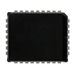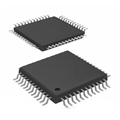
Hình ảnh chỉ để tham khảo
EF2L45BG256B
- Nhà sản xuất
- Ông. Phần #EF2L45BG256B
- Gói
- Bảng dữ liệu
- Có sẵn20800
100% gốc & amp; Mới
24 giờ sẵn sàng để vận chuyển
Bảo hành 365 ngày
RFQ & amp; Nhận thêm Giảm giá
Thông số kỹ thuật
| Manufacturer | JLCPCB Assembly |
| Package | FBGA-256 |
Tổng quan
Description
This memory chip is based on advanced 3D NAND technology, enabling higher data density, improved durability, and faster read/write speeds compared to traditional 2D NAND solutions. It supports features such as error correction, wear leveling, and power loss protection, enhancing data integrity and longevity.
The EF2L45BG256B interfaces through standard protocols like ONFI or Toggle Mode, ensuring compatibility with various controllers and systems. Its versatility makes it suitable for use in smartphones, tablets, embedded systems, and other high-demand environments where reliable and efficient data storage is essential. Overall, the EF2L45BG256B represents a modern solution for expanding memory capabilities in a wide range of electronic applications.
Features
1. Organization: It is organized as 2048 blocks of 128 pages, with each page consisting of 2048 bytes of user data plus additional spare areas for error correction.
2. Interface: The device utilizes a parallel interface, allowing for easy integration into various systems.
3. High Performance: Supports fast read and write speeds, enhancing overall data transfer efficiency.
4. Reliability: Features advanced error correction capabilities and wear leveling to extend the lifespan of the memory.
5. Low Power Consumption: Designed for energy efficiency, making it suitable for battery-operated devices.
6. Temperature Range: Operates over a wide temperature range, ensuring functionality in diverse environments.
7. Applications: Ideal for use in consumer electronics, automotive, and industrial applications requiring reliable data storage.
These features make the EF2L45BG256B a versatile choice for modern digital storage solutions.
Package
Pinout
The primary functions of the pins include:
1. Data Inputs/Outputs (DQ): 8 bits for data transfer.
2. Address Inputs (A): Used to select the memory location.
3. Control Pins (CS, RAS, CAS, WE): For controlling read and write operations.
4. Clock Input (CK): Synchronization for data transfer.
5. Power Supply (VDD, VSS): Power connections for the device.
6. Mode Register Set (MRS) and Refresh Pins: For setting operational modes and refreshing the memory.
This device supports a wide range of functionalities, including burst read/write operations, and is designed for high performance in various applications.
Manufacturer
Application
Equivalent
Vận chuyển
Phương pháp vận chuyển Chúng tôi
cung cấp dịch vụ vận chuyển toàn cầu thông qua DHL, FedEx, TNT, UPS hoặc bất kỳ nhà giao hàng khác mà bạn lựa chọn.
Tham khảo phí vận chuyển (DHL / FedEx):
Hãng DHL: Chi phí vận chuyển dao động từ $ 25- $ 45 (0,5kg), với thời gian giao hàng ước tính là 2-5 ngày làm việc.
FedEx: Chi phí vận chuyển dao động từ $ 25- $ 40 (0,5kg), với thời gian giao hàng ước tính là 3-7 ngày làm việc.
Sản phẩm UPS: Chi phí vận chuyển dao động từ $ 25- $ 45 (0,5kg), với thời gian giao hàng ước tính là 3-7 ngày làm việc.
TNT: Chi phí vận chuyển dao động từ $ 25- $ 65 (0,5kg), với thời gian giao hàng ước tính là 3-7 ngày làm việc.
EMS: Chi phí vận chuyển dao động từ $ 30- $ 50 (0,5kg), với thời gian giao hàng ước tính là 7-15 ngày làm việc.
Đăng ký Air Mail: Chi phí vận chuyển là $ 2- $ 4 (0.1kg), với thời gian giao hàng ước tính là 5-20 ngày làm việc.
Thanh toán
Payment Methods
Thời hạn thanh toán là 100% trả trước.
Hiện tại, chúng tôi chỉ chấp nhận các phương thức thanh toán dưới đây:
1. PayPal
2. Thẻ tín dụng / ghi nợ
3. Chuyển dây
Tương tự
-
![MX25R8035FM1IL0]() MX25R8035FM1IL0
Macronix
-
![MX25V1635FZNQ03]() MX25V1635FZNQ03
Macronix
-
![MX25V5126FM1I]() MX25V5126FM1I
Macronix
-
![MX25R6435FBDIL0]() MX25R6435FBDIL0
Macronix
-
![MX25L25673GMI-10G]() MX25L25673GMI-10G
Macronix
-
![MX25U51279GXDR00]() MX25U51279GXDR00
Macronix
-
![MX25U25643GZNI00]() MX25U25643GZNI00
Macronix
-
![MX25U6435FM2I-10G]() MX25U6435FM2I-10G
Macronix
-
![MX25L12833FM2I-10G]() MX25L12833FM2I-10..
Macronix
-
![MX29F040CQI-70G]() MX29F040CQI-70G
Macronix
-
![MX25L25645GXDI-08G]() MX25L25645GXDI-08..
Macronix
-
![MX25L25735FMI-10G]() MX25L25735FMI-10G
Macronix