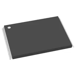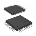
Hình ảnh chỉ để tham khảo
74LVC1G79GW
D FLIP-FLOP, LVC/LCX/Z SERIES, 1
- Nhà sản xuất
- Ông. Phần #74LVC1G79GW
- Gói
- Bảng dữ liệu 74LVC1G79GW DataSheet
- Có sẵn6437
100% gốc & amp; Mới
24 giờ sẵn sàng để vận chuyển
Bảo hành 365 ngày
RFQ & amp; Nhận thêm Giảm giá
Thông số kỹ thuật
| Package | Bulk |
| ProductStatus | Active |
Tổng quan
Description
The 74LVC1G79GW comes in a small, space-efficient package, such as the TSSOP or DFN, making it ideal for compact circuit designs. Its low power consumption and high noise immunity make it suitable for battery-powered and portable applications. Additionally, the device supports partial power-down mode, which allows it to be used in systems where power conservation is critical. Its robustness, versatility, and ease of integration make the 74LVC1G79GW a popular choice for implementing synchronous data storage elements in digital electronics.
Features
It supports a clock input that triggers on the rising edge, and it has Schmitt-trigger action inputs which provides better noise immunity. The flip-flop is capable of high-speed operation, with a typical propagation delay time of around 3.2 ns at 5 V. It comes in a leadless package type, such as TSSOP, making it suitable for compact circuit designs. Additionally, the 74LVC1G79GW provides ESD protection, which enhances its robustness in industrial and consumer applications. Overall, its compact size, wide voltage range, and efficient performance make it suitable for portable and battery-powered devices.
Package
Pinout
The pin functions are as follows:
1. Pin 1 (D): Data input. The data on this pin is transferred to the Q output on the rising edge of the clock signal.
2. Pin 2 (GND): Ground. This is the common ground reference for the device.
3. Pin 3 (CP): Clock input. The flip-flop captures the data from the D input on the rising edge of this clock signal.
4. Pin 4 (Q): Data output. This pin reflects the state of the D input after the clock signal has triggered.
5. Pin 5 (Q̅): Inverted data output. This pin provides the inverse of the data present at the Q output.
6. Pin 6 (VCC): Power supply. This pin is connected to the positive supply voltage.
The 74LVC1G79GW is commonly used in digital circuits for data storage and transfer applications.
Manufacturer
Application
Equivalent
1. SN74LVC1G79 from Texas Instruments
2. NXP's 74LVC1G79GV
3. Microchip's 74LVC1G79
4. ON Semiconductor's NL17SZ74
Ensure to compare datasheets for specific operational characteristics and package types.
Vận chuyển
Phương pháp vận chuyển Chúng tôi
cung cấp dịch vụ vận chuyển toàn cầu thông qua DHL, FedEx, TNT, UPS hoặc bất kỳ nhà giao hàng khác mà bạn lựa chọn.
Tham khảo phí vận chuyển (DHL / FedEx):
Hãng DHL: Chi phí vận chuyển dao động từ $ 25- $ 45 (0,5kg), với thời gian giao hàng ước tính là 2-5 ngày làm việc.
FedEx: Chi phí vận chuyển dao động từ $ 25- $ 40 (0,5kg), với thời gian giao hàng ước tính là 3-7 ngày làm việc.
Sản phẩm UPS: Chi phí vận chuyển dao động từ $ 25- $ 45 (0,5kg), với thời gian giao hàng ước tính là 3-7 ngày làm việc.
TNT: Chi phí vận chuyển dao động từ $ 25- $ 65 (0,5kg), với thời gian giao hàng ước tính là 3-7 ngày làm việc.
EMS: Chi phí vận chuyển dao động từ $ 30- $ 50 (0,5kg), với thời gian giao hàng ước tính là 7-15 ngày làm việc.
Đăng ký Air Mail: Chi phí vận chuyển là $ 2- $ 4 (0.1kg), với thời gian giao hàng ước tính là 5-20 ngày làm việc.
Thanh toán
Payment Methods
Thời hạn thanh toán là 100% trả trước.
Hiện tại, chúng tôi chỉ chấp nhận các phương thức thanh toán dưới đây:
1. PayPal
2. Thẻ tín dụng / ghi nợ
3. Chuyển dây
Tương tự
-
![MX25L3233FM1I-08Q]() MX25L3233FM1I-08Q
Macronix
-
![MX25V1635FZNQ03]() MX25V1635FZNQ03
Macronix
-
![MX66U1G45GXDI00]() MX66U1G45GXDI00
Macronix
-
![MX25V4035FZUI]() MX25V4035FZUI
Macronix
-
![MX25V16066M2I02]() MX25V16066M2I02
Macronix
-
![MX30LF2G28AD-TI]() MX30LF2G28AD-TI
Macronix
-
![MX25R6435FBDIL0]() MX25R6435FBDIL0
Macronix
-
![MX25L2006EM1I-12G]() MX25L2006EM1I-12G
Macronix
-
![MX25L6433FM2I-08G]() MX25L6433FM2I-08G
Macronix
-
![MX25L12833FM2I-10G]() MX25L12833FM2I-10..
Macronix
-
![MX25U25645GXDI00]() MX25U25645GXDI00
Macronix
-
![MX29LV160DTTI-70G]() MX29LV160DTTI-70G
Macronix