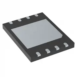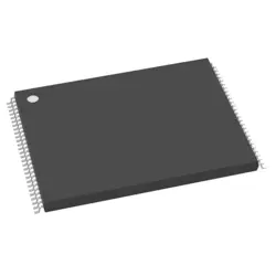
Hình ảnh chỉ để tham khảo
74LVC1G126GW
Buffers & Line Drivers
- Nhà sản xuất
- Ông. Phần #74LVC1G126GW
- Gói
- Bảng dữ liệu
- Có sẵn9210
100% gốc & amp; Mới
24 giờ sẵn sàng để vận chuyển
Bảo hành 365 ngày
RFQ & amp; Nhận thêm Giảm giá
Thông số kỹ thuật
Tổng quan
Description
Key specifications include a supply voltage range of 1.65V to 5.5V, making it suitable for various logic levels, including 3.3V and 5V systems. The device operates at high speeds with a propagation delay of around 3.5 ns at 3.3V. The input and output are compatible with standard LVC logic levels, ensuring broad usability in digital designs.
The package type, GW, indicates a small footprint, which is ideal for space-constrained applications. Typical use cases include signal buffering, level shifting, and bus driving in microcontroller and FPGA interfaces. Overall, the 74LVC1G126GW is a versatile component for modern electronic designs requiring efficient signal management.
Features
1. Voltage Range: Operates from 1.65V to 5.5V, making it suitable for various low-voltage applications.
2. Low Power Consumption: Offers low static and dynamic power consumption, ideal for battery-operated devices.
3. High-Speed Operation: Supports fast switching times, enhancing performance in high-speed applications.
4. Three-State Outputs: The outputs can be placed in a high-impedance state, allowing for bus-oriented applications and reducing loading on shared lines.
5. Input Compatibility: Compatible with TTL (Transistor-Transistor Logic) levels, enabling easy interfacing with other logic families.
6. ESD Protection: Provides robust electrostatic discharge protection, ensuring reliability in harsh environments.
7. Small Package: Available in compact packages (e.g., SC-70), facilitating space-saving designs.
This versatile device is widely used in signal buffering, level shifting, and interfacing applications.
Package
Pinout
1. A (Input): This is the data input pin.
2. OE (Output Enable): Controls the output state. When enabled, the output reflects the input state; when disabled, the output is in high-impedance.
3. Y (Output): This is the buffered output pin that reflects the input state when the output is enabled.
4. VCC (Power Supply): The supply voltage pin, typically ranging from 1.65V to 5.5V.
5. GND (Ground): The ground connection pin.
The device is commonly used in digital circuits for signal buffering and level shifting, providing a way to control the flow of signals while ensuring the output can be disabled when not in use.
Manufacturer
Application
Equivalent
Vận chuyển
Phương pháp vận chuyển Chúng tôi
cung cấp dịch vụ vận chuyển toàn cầu thông qua DHL, FedEx, TNT, UPS hoặc bất kỳ nhà giao hàng khác mà bạn lựa chọn.
Tham khảo phí vận chuyển (DHL / FedEx):
Hãng DHL: Chi phí vận chuyển dao động từ $ 25- $ 45 (0,5kg), với thời gian giao hàng ước tính là 2-5 ngày làm việc.
FedEx: Chi phí vận chuyển dao động từ $ 25- $ 40 (0,5kg), với thời gian giao hàng ước tính là 3-7 ngày làm việc.
Sản phẩm UPS: Chi phí vận chuyển dao động từ $ 25- $ 45 (0,5kg), với thời gian giao hàng ước tính là 3-7 ngày làm việc.
TNT: Chi phí vận chuyển dao động từ $ 25- $ 65 (0,5kg), với thời gian giao hàng ước tính là 3-7 ngày làm việc.
EMS: Chi phí vận chuyển dao động từ $ 30- $ 50 (0,5kg), với thời gian giao hàng ước tính là 7-15 ngày làm việc.
Đăng ký Air Mail: Chi phí vận chuyển là $ 2- $ 4 (0.1kg), với thời gian giao hàng ước tính là 5-20 ngày làm việc.
Thanh toán
Payment Methods
Thời hạn thanh toán là 100% trả trước.
Hiện tại, chúng tôi chỉ chấp nhận các phương thức thanh toán dưới đây:
1. PayPal
2. Thẻ tín dụng / ghi nợ
3. Chuyển dây
Tương tự
-
![MX25R8035FM1IL0]() MX25R8035FM1IL0
Macronix
-
![MX25L3233FZBI-08Q]() MX25L3233FZBI-08Q
Macronix
-
![MX25V1635FZNI]() MX25V1635FZNI
Macronix
-
![MX29F400CBTI-70G]() MX29F400CBTI-70G
Macronix
-
![MX25V16066M2I02]() MX25V16066M2I02
Macronix
-
![MX25U51279GXDR00]() MX25U51279GXDR00
Macronix
-
![MX25U25643GZNI00]() MX25U25643GZNI00
Macronix
-
![MX25U6435FM2I-10G]() MX25U6435FM2I-10G
Macronix
-
![MX25L12833FM2I-10G]() MX25L12833FM2I-10..
Macronix
-
![MX25L12833FZNI-10G]() MX25L12833FZNI-10..
Macronix
-
![MX25L12835FZ2I-10G]() MX25L12835FZ2I-10..
Macronix
-
![MX29LV160DTTI-70G]() MX29LV160DTTI-70G
Macronix